Developing high-throughput methods to characterise graphene
Challenge
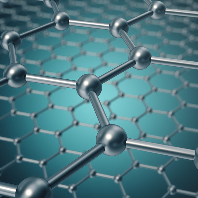
Graphene is a lattice of carbon only one atom thick. Despite being effectively two-dimensional (2D) it is the strongest material ever discovered with a tensile strength over 200 times stronger than structural steel. It also has the lowest room-temperature electrical resistivity of any known material and its high electron mobility – which is how quickly electrons can move through it – would allow electronic devices to operate at much higher frequency ranges. These attributes open the possibility for its use as a new material in the electronic industry and for composite materials.
However, the inability to grow large areas of graphene with sufficient purity and with uniform and reproducible electric and electronic properties has restricted its uptake by industry. This issue has been highlighted by standard organisations such as the International Electrotechnical Commission (IEC) and the European Committee for Electrotechnical Standardisation (CENELEC), that initiated working groups such as IEC/TC113 to address this problem.
A major hurdle to producing high-purity graphene was a lack of validated high-throughput, non-contact characterisation methods, such as optical based instrumentation, for use on test samples or in-line in an industrial environment. Many of these methods, such as scanning probe microscopy, microwave resonant cavity and time-domain THz waves spectroscopy (THz-TDS) posed problems in practical application to an atomically thin material such as graphene. These non-contact methods lacked verification of the underlying assumptions, traceability to the SI, and the expression of the measurement uncertainty.
In addition, fluctuations in ambient conditions, such as temperature and humidity, affect the electrical properties of graphene, resulting in differences between measurements at different locations. Therefore, the uncertainty, accuracy and reliability of the measurements using such non-contact methods were unknown.
Solution
Prior to the EMPIR project Developing electrical characterisation methods for future graphene electronics no metrological inter-laboratory comparison of the electrical properties of graphene had been performed in terms of comparing the measurements from different methods.
During the project 45 graphene samples were characterised for conductivity, electron mobility, carrier density and effect of environmental conditions on measurements. To achieve this the project consortium performed extensive validation on a range of contact methods, including the van der Pauw method and, for the first time, Electrical Resistance Tomography, providing traceability to the SI for these techniques.
Once validated these contact methods were then compared with potential non-contact methods already employed for analysing thin film materials. In particular, a promising non-contact, high-throughput method using THz-TDS was examined. This technique measures the change in shape of picosecond-duration electromagnetic pulses over time that are either reflected from or transmitted through the sample to give information on its electrical properties.
The results exhibited excellent agreement between the different techniques and highlighted the need for standardised electrical measurements in highly controlled environmental conditions and the application of appropriate weighting functions.
Impact
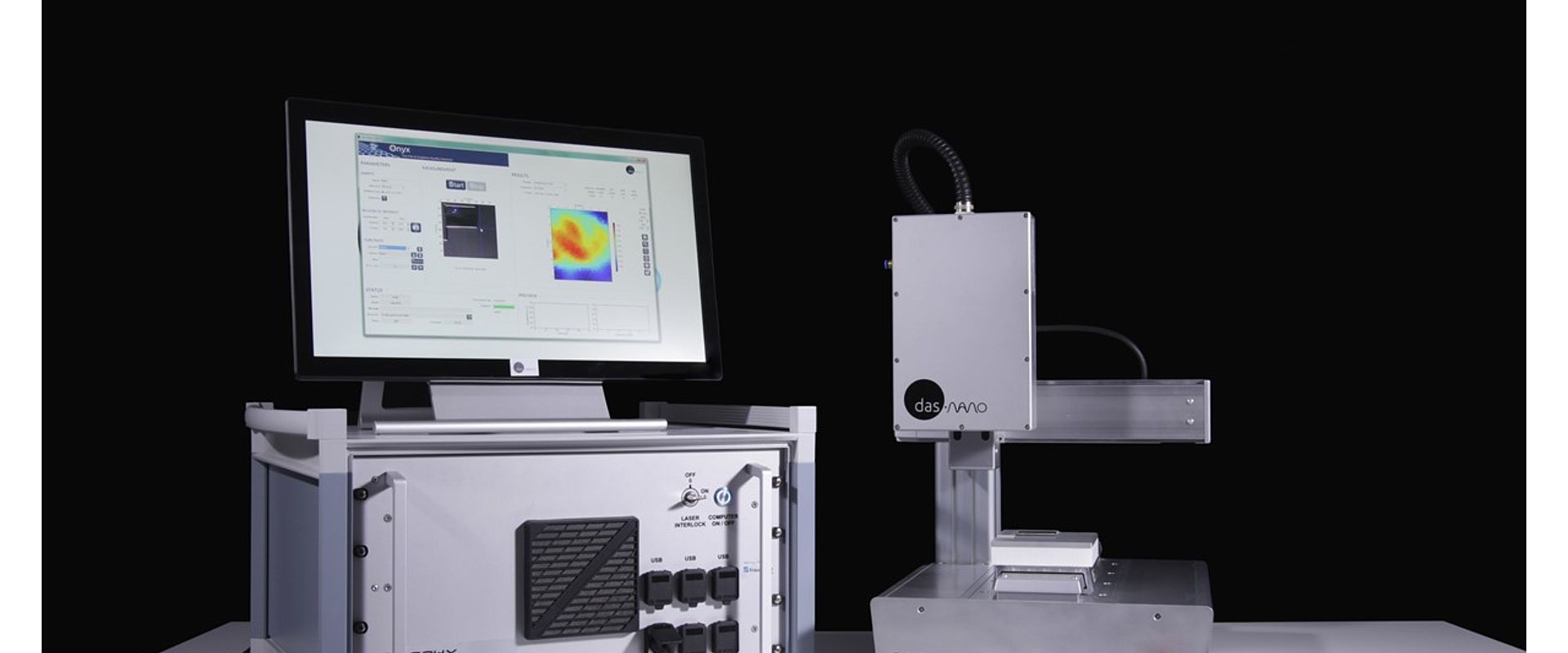
Project partner Das-Nano is a technological-based company that solves industrial problems for the automotive, advanced materials, wind energy and aerospace sectors. Das-Nano provided the ONYX THz-TDS optical system that was validated in the interlaboratory comparison.
As a result of the project Das-Nano now has data from top metrology institutes in Europe supporting the use of THz-TDS for the electrical characterization of graphene, information it can pass on to its customers. The ONYX instrument allows a full-area, non-destructive characterization of Graphene, thin films, and other 2D materials over a large scale, from the sub-millimetre to the m2 level, providing information of a range of parameters in a single measurement. This includes data on a sample’s refractive index, electrical resistivity, charge carrier mobility and charge carrier density.
The use of high-throughput, accurate characterisation measurements using THz technology will allow industry to perform accurate measurements on the electrical properties of graphene. This will provide customers with reliable and comparable specifications of graphene as an industrial product, allowing the development of such things as more efficient solar panels and electronics, advanced batteries, and composite materials for health and aerospace.
- Category
- EMPIR,
- Standardisation,
