Expanding European capability in small-scale magnetic field measurements
Challenge
Technology based on the ‘Hall effect’, which determines magnetic field strength by measuring the voltages induced by electric current, accounted for more than 50% of the €1.7 billion global market for magnetic sensors in 2019. Magnetic measurements are important to ensure the correct placement of batteries or device performance in a range of modern technologies, including consumer electronics, induction chargers and electric cars. Many of these require magnetic field measurements at the micro or nanometre scale and whilst techniques were established for measuring homogeneous fields at this level none existed for spatially varying ones. Small, varying magnetic fields are not only weak, with field strength decreasing with increasing distance from a sample’s surface, but can also change direction and interact with other fields in close proximity, complicating measurements. One suitable measurement technique is ‘Scanning Hall Microscopy’ which utilises a small micro or nanometre sized semi-conductor Hall sensor. The small sensor size and low measurement height avoids averaging measurements over fields pointing in different directions with a high spatial resolution and mathematical analysis of the results reveals features of the magnetic fields. However, SI traceability did not exist for this technique at the required scale, restricting its uptake by European industry.
Solution
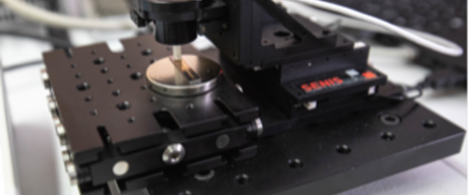
During the EMPIR project Nano-scale traceable magnetic field measurements, project partner SENIS AG developed more than a dozen Scanning Hall Mappers using Complementary metal–oxide–semiconductor (CMOS) technology that ranged in size and spatial resolutions. This resulted in the development of a high-resolution nano-Hall mapper with a 50-nanometre positioning accuracy and a 1000 nanometre spatial resolution. Capable of a large scan range of several centimetres the new mapper features a compact Hall probe with a field sensitive volume of 10 micrometres x 10 micrometres x 10 micrometres, which is an order of magnitude smaller than any commercially available magnetic sensor. The new mapper can measure fluctuating magnetic fields with a 3D positioning resolution at the 50-nanometre level with a minimum field resolution better than 5 μT. The system was traceably calibrated at SENIS’s accredited laboratory and its performance validated using an electromagnet provided by PTB, Germany’s National Metrology Institute (NMI).
Impact
Founded in 2004, SENIS provides research and development solutions for magnetic and electric field measurements. It also develops and manufactures its own sensors in its certified calibration facilities. Around 95% of the company’s products are based on Hall probes and SENIS is one of the few companies providing certified magnetic measurements that can be traced back to national standards. Prior to SENIS’s participation in the project the company was the sole producer of instruments for measuring 3D magnetic fields at the micrometre scale. Now, through participation in the project these have been reduced in size by a factor of ten with project results integrated into its commercial nano-Hall mapper. As well as the development of a new commercial product SENIS now has knowledge of the limits of this technology, such as the workable size for Hall probes, information it can pass on to customers. For the first time the capability exists in Europe for measuring fluctuating magnetic fields at the micro and nano scale level, essential to support the high technology industries of the future and help maintain Europe’s position in the global market for magnetic sensors.
- Category
- EMPIR,
- SI Broader Scope / Integrated European Metrology,
