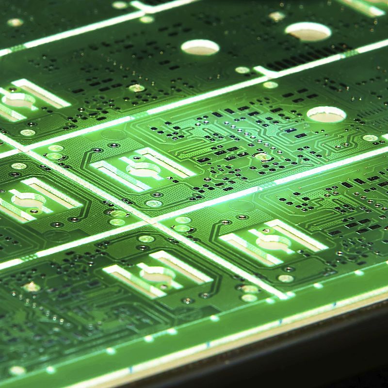
Measurements for high speed production
Challenge
The manufacture of many low-value items is being outsourced to countries outside of Europe. In response European manufacturers are repurposing high-throughput processes, such as printing and injection moulding, to produce high-value devices, recognising the [potential] ‘economy of scale’. Roll-to-roll (R2R) manufacturing is an established platform for the mass production of a range of film-type products where multiple copies can be printed simultaneously using rollers. This is now being applied to the manufacture of integrated circuits, solar cells and ‘smart packaging’ and has the advantage that multiple layers of different materials can be overlaid during printing.
Many of these items, such as printed circuits, contain nanometre sized components the correct alignment or ‘registration’ of which on, and between, layers is critical to product performance. Measurements to ensure registration must be accurate, fast and made in-line during production to allow defects to be detected at an early stage and criteria are tightening as designers look to further miniaturise their devices. Stakeholders in the R2R sector have stated that an overlay registration accuracy of ± 20 μm is the target required for promoting this technology but the current state of the art for this measurement was ± 50 μm.
Solution
The EMPIR project Metrology for highly-parallel manufacturing not only achieved a 1- 5 μm measurement accuracy for detecting registration error but also a ± 20 µm overlay accuracy, an improvement on the current state-of the-art and the target identified as vital by stakeholders.
This was accomplished by project partners VTT and Offcode, who developed a new system for handling large-area substrates. This comprised integrating ‘registration mark metrology’, where alignment markings are printed onto the various layers using a cylinder, with in-line feedback from a high-resolution camera to verify the alignment accuracy. The process was then optimised for detecting errors by taking into account contributions from the substrate, the printing hardware, printed registration marks and the accuracy of the instrumentation itself. The system was then verified for use with different printing materials and different process speeds.
Impact
Offcode, an engineering firm located in Oulu, Finland specializes in integrating electronics into larger systems and, as well as helping their customers to implement and coordinate complex, multiple technologies, they also provide measurement instruments for R2R production lines.
Offcode’s advanced ARCOS camera for printing machines formed the basis of the novel registration system developed in the project. As a result of participation this system was improved and can now detect registration errors down to 1 μm. Offcode has sold a number of these upgraded cameras since the end of the project but the company considers that the greatest benefit from the work was the knowledge gained, which they can now include in the other products and services they deliver to their customers.
The manufacturing techniques developed, and the increase in measurement accuracy achieved for substrate alignment and verification as a result of the project, will help further reduce the cost of production of European goods. This in turn will lead to a stronger manufacturing base in Europe.
- Category
- EMRP,
- Industry,
